S. S. Oluyamo*
Department of Physics, Federal University of Technology, Akure, Nigeria. E-mail: oluyamos@yahoo.com
DOI : http://dx.doi.org/10.13005/msri/080203
Article Publishing History
Article Received on : 03 Apr 2011
Article Accepted on : 09 May 2011
Article Published :
Plagiarism Check: No
Article Metrics
ABSTRACT:
The study investigates the effects of surface area on the electrical properties of tellurium thin films for electric field values 0.05 – 0.50V/m. Different areas of the films were prepared by vacuum evaporation method at a pressure of 5×10⁻⁵torr. Measurements of current – voltage characteristics were obtained at room temperature. The areas of the films were found to affect the electrical properties of the films. The surface conductance of the films decreases with increase in area while the saturation current density increases with increase in area. The reduction in surface conduction could be attributed to larger resistance imposed by films of larger areas. However, the study revealed that there is little variation in the values of the barrier heights of the samples. Therefore within the limit of the study, surface area has no significant effect on the barrier height of tellurium thin films.
KEYWORDS:
Surface area; Tellurium; Electrical properties
Copy the following to cite this article:
Oluyamo S. S. Effects of Surface Area on the Electrical Properties of Tellurium Thin Films. Mat.Sci.Res.India;8(2)
|
Introduction
Tellurium is a semiconducting element with very wide application in electronic and metallurgical works. This is because; Tellurium sometimes behaves like metals with high density of state at the fermi level. It also exhibits different behaviours in liquid and solid states (Grove, 1968; Orma, 1975; Thurn and Rusica, 1975; Sze, 1985). Studies had been carried out on the electrical behaviour of this material at various stages which indicate that the shape of the current–voltage characteristics is symmetrical in both the forward and backward directions (Kittel, 1985; Van Vechten, 1970).
Studies had shown that various factors such as probe shapes, temperature, humidity, pressure etc, have effects on the conducting behaviour of semiconducting thin films (Owate and Akpata, 1998; Oluyamo, 1999 and 2003; Oluyamo and Ojo, 2004; Alamri and Brinkman, 2000). Phahle (1977), reported on the electrical conductivity, hall voltage, and thermoelectric power of vacuum deposited tellurium thin films. The study showed that the films were p-type with crystalographic defects providing additional acceptor centres. Terminal assisted hopping conduction was also found to be predominant at temperature below 150K.
The present study investigates the effects of surface area on the electrical properties of tellurium films as most devices for electrical, electronic and metallurgical works depend to a large extend on the shape of the material. The area of films is also known to be a major factor in the manufacture and assemblage of electrical and electronic devices. The desired shapes of the films were generated using mica mask while the nature of the configuration was determined using the current–voltage characteristics at room temperature.
Experimental
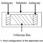
The mica mask used to generate the required design were washed with soap detergent and rinsed with water. This was followed by ultrasonic agitation in deionised water, acetone, and ethyl alcohol for twenty minutes each. The polished glass slides that were used as substrates were first boiled in chromic acid and ultrasonically cleaned as described for mica mask above. The substrates (glass slides) were then enclosed in a vacuum chamber (Edward coating Unit model 306) and tellurium films of thickness 1000A0 were deposited on the substrate from a tungsten filament at a pressure of 5×10⁻⁵torr. Electrical contacts were made to opposite ends of the films by depositing Sb metal on the electrode width. All the evaporant were of 5N9 purity. The final configuration of films is shown in fig. 1. The current–voltage characteristics of the samples were measured with a digital electrometer (Keittley, type 160B) and a digital multivoltmeter (Hewlett – Packard type 3465A) at room temperature.
Figure 1: Final configuration of the deposited samples
Results and Discussion
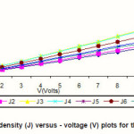
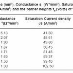
Figure 2 shows plots of current density (J) and the Voltage (V) measurements for all the samples. The current in the samples increases with increase in voltage. In addition, the samples show linear J–V relationship over the voltage range 0.05–0.50V. The values of the surface conductance, saturation current density and the barrier heights of the samples are recorded in table 1. The conductance of the samples decreases with increase in surface area while the saturation current density increases with increase in surface area. The decrease in conductance with increase in area could be attributed to larger resistance imposed by films of larger areas thereby resulting to increase in saturation current density. However, only little variations were observed in the values of the barrier height of the samples. The results in this study are in agreement with previous works by Oberafo et al (1994); Oluyamo (1999 and 2003) for Bi/Te, Sb/Te and Sb/Si contacts respectively.
Figure 2: Current density (J) versus – voltage (V) plots for the eigth samples
Table 1: Area (mm2), Conductance s (W-1/mm2), Saturation current density Js (A/mm2) and the barrier heights fB (Volts) of the Samples
The conductance of the samples were calculated from the slope of the best line of fit of the current density – voltage plots (fig2) and using the relationship,
J = σV (Arthur, 1983; Sze, 1985; Oluyamo and Babalola, 2006). Where s is the conductance of the samples and obtained from the best line of fit of the J–V plots.
The barrier heights were calculated from the current–voltage forward characteristics using the thermionic emission theory with the current – voltage relationship given as;
J = Jσ (exp (qV/kT) – 1). V is the voltage across the device terminals.
For negligible series resistance;
Js = A**T2exp {-qφB}
kT
Where A** is the Richardson constant, φB
is the zero field asymptotic barrier height, k, the Boltzmann’s constant, T, the absolute temperature and q, the magnitude of the electronic charge.
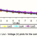
Figure 3 shows the LnJ – Voltage plots for the samples. This figure gives curves which is expected at the region V<3kT/q for the study. The values of the saturation current density Js were obtained from the extrapolated LnJ to zero voltage. The barrier heights were also estimated using the relationship,
φ =Kt/qLn(A**T²)/Js
Figure 3: LnJ-Voltage (V) plots for the samples
Conclusion
The current in all the samples increases with increase in voltage. Hence, the samples are ohmic within the voltage range 0.050 – 0.50V. The conductance reduces with increase in the area of the films while the saturation current density wasfound to increase with increase in the area of films.This could be due to the fact that films with larger areas create higher resistance thereby, reducing the conductance, which results to increase in saturation current density. However, the study revealed that there exist little variation in the values of the barrier heights of the samples. The study agrees with previous works by Oberafo et al (1994), Oluyamo (1999 and 2003) for Bi/Te, Sb/Te, Sb/Si contacts respectively.
References
- Alamri, S. N. and Brinkman, A. W., The effect of the transport conductive oxide on the performance of thin film CdS/Cde solar cells.Journal of Physics, D: Applied Physics, 33: 11-14 (2000).
CrossRef
- Arthur, Kip F., Fundamentals of Electricity and magnetism. MC Graw Hill International Book company, Japan Pp165 – 168 (1984).
- Grove, A. S., Physics and Tecnology of Semiconductor Devices. John Wiley and Sons Inc. Pp 55-60 (1968).
- Kittel, C.. Introduction to Solid State Physics. John Wiley and Sons Inc. London. Pp 230 – 245 (1985).
- Oberafo, A. A. Odunaike, R. K.and Mukolu,A. I., The behaviour of Bi matal contact to Te films. International Journal of Biochemiphysics, 3: 78-81 (1994).
- Oluyamo, S. S., Effects of Probe Shapes on the barrier height and Surface Conductance of Tellurium thin films, Pakistan Journal of Sciencetific and Industrial Research, 2(3): 113-116 (1999).
- Oluyamo, S . S. and Ojo J. S., Elevated Temperature effects on the conduction Properties of Bi metal contacts to Si thin films.Global Journal of pure and Applied Sciences, 10(1): 217-221 (2004).
- Oluyamo, S. S., Electrical properties of Sb metal contacts to Si thin films. Nigeria Journal of Pure and Applied Physics, 2: 40-44 (2003).
CrossRef
- Oluyamo, S . S. and Babalola, I. A., Electrical properties in Al/Bi/Ge alloy systems. Material Science Research India, 3: (1a): 55-58 (2006).
CrossRef
- Ormar, M. A., Elementary Solid State Physics, Addison Wesley Publishing Company, London. Pp 286 – 290 (1975).
- Owate, I. O. and Akpata, A. N. O., The degredation of Silicon Semiconductor materials in various media. Nigeria Journal of Physics, 10: 75-78 (1998).
- Phale, A. M., Electrical conductivity, Hall voltage and thermoelectric power of vacuum deposited tellurium films. Thin Solid Films, 45: 235 – 240 (1977).
- Sze, S. M., Physics of Semiconductor Devices, John Wiley and Sons, London Pp63-403 (1985).
- Thurn, H and Rusica, J., Change of bonding system in liquid Se-Te alloys as shown by density measurements. Journal of non crystalline solids, 35(36): 1263-1267 (1975).
- 15. Van Vechen, J. A. and Bergstresser, T. K.,Electronic Structures of Semiconductor Alloys. Physical Review, 8: 3351 (1970)
CrossRef
Views: 221
 This work is licensed under a Creative Commons Attribution 4.0 International License.
 Material Science Research India An International Peer Reviewed Research Journal


